The SG3525A is a high-performance pulse width modulator (PWM) controller integrated circuit designed for power supply and motor drive applications. This versatile chip offers precise control over switching frequencies and duty cycles, making it ideal for various power conversion systems. It operates within a supply voltage range of 8V to 35V and features a built-in 5.1V reference voltage, allowing for precise regulation of output voltage. This IC is ideal for applications such as DC-DC converters, inverters, and motor speed control, offering improved performance with fewer external components. Its advanced features, including soft-start circuitry and adjustable dead time, enhance reliability and efficiency in power management systems.
Key Features:
- Wide input voltage range: 8V to 35V
- Adjustable switching frequency: 100 Hz to 400 kHz
- Dual totem-pole outputs for direct drive of power MOSFETs
- Built-in soft-start circuitry
- Under-voltage lockout protection
- Programmable dead-time control
- 5.1V reference trimmed to ± 1%
- Pulse-by-pulse shutdown capability
- Separate oscillator sync terminal
Technical Specifications:
| Specification | Value |
|---|---|
| Supply Voltage | 8V to 35V |
| Supply Voltage VCC | +40 Vdc |
| Oscillation Range | 100 Hz to 400 kHz |
| Reference Voltage | 5.1 V trimmed to ±1% |
| Logic Input | -0.3V to 5.5V |
| Output Current IO | ±500 mA |
| Reference Output Current Iref | 50 mA |
| Oscillator Charging Current | 5 mA |
| Maximum Power Dissipation | 1000 mW |
| Thermal Resistance (Junction-to-Air) | 100 °C/W |
| Thermal Resistance (Junction-to-Case) | 60 °C/W |
| Operating Junction Temperature | 150 °C |
Applications:
- Switch-mode power supplies (SMPS)
- DC-DC converters
- Motor drive controls
- Solar inverters
- Uninterruptible power supplies (UPS)
- Lighting control systems
- Audio amplifiers
- Battery charging systems
Pinout Diagram:
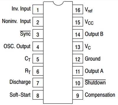
The Function of SG3525A Pin
| Pin Number | Pin Name | Pin Function |
|---|---|---|
| 1 | INV | Inverting Input |
| 2 | NINV | Non-Inverting Input |
| 3 | SYNC | Synchronizing IC with an external oscillator frequency |
| 4 | OSC. Output | Oscillator Output. The frequency of IC is confirmed at this pin |
| 5, 6 | CT & RT | These pins are used to connect an external capacitor and resistor, respectively, to set up the frequency of the oscillator circuit |
| 7 | Discharge (DIS) | This pin is used to determine the dead time for IC. A resistor connected between pins 7 and 5 decides the frequency of PWM (or dead time) |
| 8 | Soft Start (SS) | A capacitor is connected to this pin and ground. It initiates operation softly |
| 9 | Compensation (COMP) | A compensation pin used to compensate for errors and avoid rapid fluctuations |
| 10 | Shutdown | A shutdown pin that narrows down PWM signals to the maximum level when set high. Used to shut down the IC’s output in the event of malfunction or unwanted condition |
| 11 | Output A | Output pin used as an input for external devices |
| 12 | VSS | Ground pin |
| 13 | VC | Power pin used to supply input voltage (5-35 V). Connected to a resistor that determines the magnitude of the trigger current to the output current |
| 14 | Output B | Output pin used as an input for external devices |
| 15 | Vin | Supply input voltage (8-35 V) |
| 16 | Vref | Reference pin used to set reference voltage through pins 1 and 2 |
Resources:


Reviews
There are no reviews yet.